- Ceramic Bearings
- Ceramic Balls and Beads
- Cutting Tools
- Ceramic Rings
- Porous Ceramic
- Structure / Components
- AlN Ceramic
- Ceramic Pipe / Tube
- Ceramic Substrates
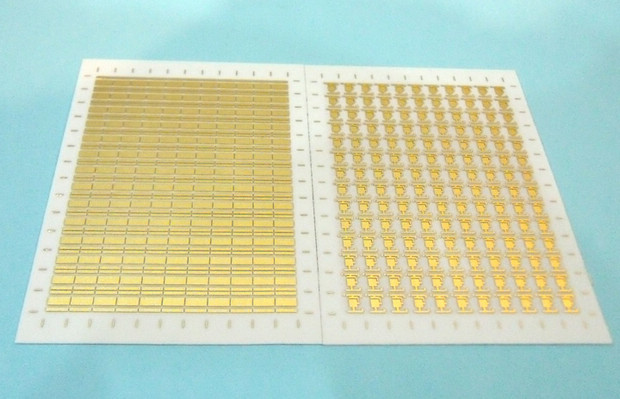
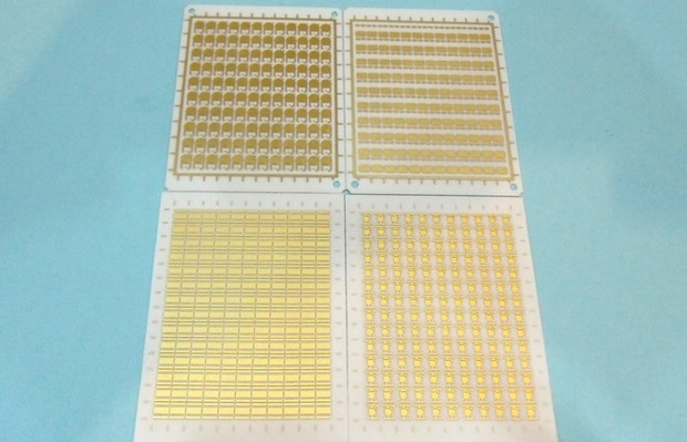
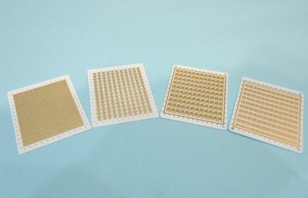
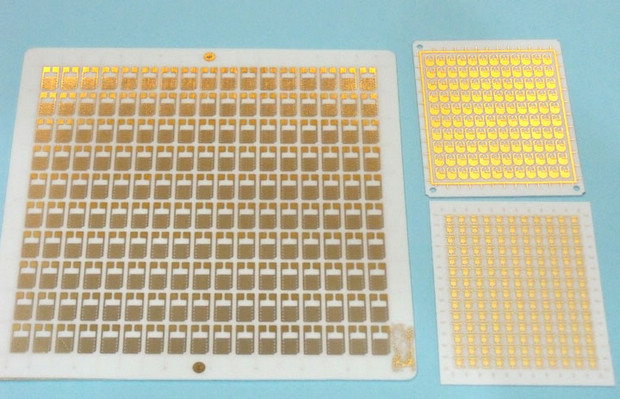
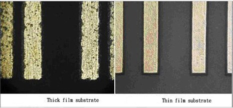
Difference between thin & thick film patterns |
|
Thin Film Patterns |
Thick Film Patterns |
Better pattern accuracyof +/-1% |
Normal Pattern accuracyof +/-10% |
Higher surface roughness of <0.3um |
Poor surface roughness of 1~3um |
Goodsurface adhesion in both Al2O3 and AlN |
Good surface adhesion in Al2O3 but poor adhesion in AlN |
Good alignment accuracy |
Poor alignment accuracy |
Higher materialstability (Cu layer) |
Normal materialstability (Ag and glass mixture) |
Conductivity Comparison of Various Materials |
|
Materials |
Conductivity(W/mK) |
FR4 |
0.2 |
Al2O3 |
17-27 |
Aluminium Nitride(AlN) |
160-230 |
Gold |
315 |
Silver |
425 |
Copper |
398 |
Ceramic metallized: Ti/W,gold(Au), sliver(Ag), Copper(Cu), nickel(Ni)¡K others & produce final circuit
- coating:0.03um to 5mil
- Ceramic Metallized substrate:
- Al2O3 substrate metallized
- AlN substrate metallized
- Silicon wafer metallized
- LED heat-dissipation ceramic substrate:
- LED Al2O3 thin film substrate
- LED Al2O3 thick film substrate
- LED AlN thin film heat-dissipation substrate
- Flip chip substrate
- The integration of the thin film,thick film,electrode plating and electroless plating processes:
Application:
1. High Power LED ceramic substrate
2. Microwave (Wireless Communication & Radar)
3. Semiconductor Process Equipment
4. Solar Cell
5. Hybrid Electric Vehicles
6. Flip chip/eutectic substrate
7. Sensor ceramic substrate
